
Recent Research Projects
Electrostatic Discharge (ESD)
Electrostatic Discharge is one of the important topics for system-level design. ESD robustness needs to be tested and reviewed for components and systems to allow safe handling and mounting in an ESD protected area. The topic of ESD projects in Missouri S&T EMC Laboratory can be on-chip ESD protection characterization, off-chip ESD protection design or combined.
ESD to Integrated Circuits (ICs)
Electrostatic Discharge(ESD) events can result in soft failures and hard failures to the integrated Circuit(ICs). To protect the ICs from ESD, ESD protection structure is critical for chip-level design. Generally, on-chip ESD protection has already been designed by the IC vendor. For off-chip ESD protection designers, the model of on-chip ESD protection is needed in order to determine the required level of off-chip ESD protection.
The most general ESD protection for IOs is the dual-diode structure with VDD-VSS power clamp. Due to the limit of port connection for ICs, three ports, including VDD-VSS, IO-VSS and IO-VDD, are all needed to be utilized to obtain all the IV-curves and the corresponding transient waveform using Transmission Line Pulse(TLP) Test. A board with a separated ground is designed to include all the connections in one board. The method uses VNA, TDR, TLP and VF-TLP to characterize the small signal model and large signal model for all ESD protection diodes.


PCB Board design(Left: Top View, Right: Middle Layer/GND Layer) to include all three connections in one board for TLP test.


TLP and VF-TLP setup diagram

On-chip ESD protection structure diagram

TLP system setup
Modeling ESD Protection Device
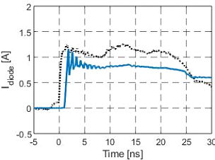
Protection devices like transient voltage suppression (TVS) diodes are often added to a circuit to improve its immunity to electrostatic discharge (ESD). Ensuring the TVS diode turns on during an ESD event, and the on-chip protection device does not take the entire charge can be challenging, however, as many on-chip ESD protection structures will turn on faster and at lower voltages than the off-chip TVS. This work developed a method to predict the system’s response to a more complicated scenario – when an ESD gun discharges to the pin of a USB cable connected to a test board which contains an IC protected by a TVS diode. The method used a hybrid simulation technique where the interactions between the ESD gun, cable, and enclosure were captured with a 3D full-wave model, and the response of the TVS and on-chip diode were captured with a SPICE model. Engineers can use this method to evaluate and optimize their ESD protection strategies’ effectiveness in a more complicated scenario.

ESD gun contact discharge to ESD protection devices through a USB cable.

SEED modeling framework for ESD protection devices


TVS current. Measured – dashed line; simulated – solid line
On-chip diode current. Measured – dashed line; simulated – solid line
On-chip diode voltage. Measured – dashed line; simulated – solid line