Recent Research Projects
Radiated Emissions
Radiated Emissions (RE) of the electronic products needs to be controlled to avoid interference with other devices. Standards for the RE compliance test such as FCC CFR Part 15 and CISPR 32 have specified the limit lines of the radiated emission for an electronic product to pass before the final release. Understanding the RE standards and investigating the controlling/mitigating methods on the RE of a product are essential to help the product pass the compliance test with enough margins and keep low risk of interfering other devices.
RE Testing Standards
The goal in this direction is to understand the RE standard and testing methods, analyze the limitations/challenges on the current RE compliance test and propose improvements corresponding to the challenges. Based on the radiated emissions of a router system with many optical modules operating above 10 GHz as the device under test, parameters that affect the accuracy of the radiated emissions are studied. In summary, there are three aspects that can be improved to increase the accuracy/confidence of the RE test or reduce the test cost: 1) possibility of missing the peak of maximal E field; 2) prediction on the number of representative modules to represent the total radiation of the fully loaded system; 3) falloff factor between the measured E field or the specified limit line at different distances such as 1 m, 3 m or 10 m. In addition, a new limit line may be needed if the 30 years-old RE compliance test standard is invalid for modern Class A devices operating above 10 GHz, such as router systems in data centers. The extraction method on a new RE limit line above 10 GHz based on the modern systems and wireless communication services such as 5 G services will be continuously under investigation by the EMC Laboratory, Missouri S&T.
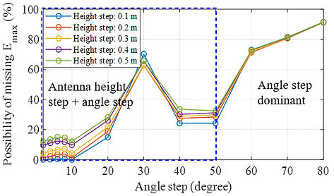
Possibility of missing the peak of maximal E field during RE scan
Power Integrity of 2.5D and 3D IC Systems
In 2.5D and 3D IC systems, the power distribution network normally consists of many layers of power/ground (P/G) grids and P/G TSVs as interconnection between the P/G layers. The impedance of the on-die PDN depends on the P/G grid, P/G TSVs and P/G grid in the silicon interposer. As there will be hundreds or thousands of P/G TSVs embedded in the 2.5D/3D IC, the equivalent capacitances from the TSVs will play an important role on the total impedance. The goal of the power integrity analysis of this research is to model the PDN impedance in the system with 2.5D/3D IC from on-die P/G grid and TSVs to the P/G plane on PCB. The influence of bias-dependency and temperature-dependency of the TSVs on the impedance of the system PDN will be investigated to illustrate that variations on the bias voltage and temperature could not be neglected to cause power integrity issues in the 2.5D/3D IC systems. Design guidelines on the on-die PDN to reduce the risk of such issues will be continuously under investigation by Missouri S&T EMC Laboratory.

Voltage and temperature dependency of the TSV capacitance
Controlling Radiated Emissions
On a vehicle, the branches on harness connected to the Engine Control Unit (ECU) carry common mode currents, which are responsible for the radiated emissions in the system level EMI test. The CISPR 25 standard testing costs much time and effort, so our goal is mimicking CISPR 25 standard testing setup to predict the EMI performance on both horizontal & vertical polarizations through component level tests, which would improve the efficiency of product development.
A procedure divided into five parts was proposed to predict radiated emissions from the harness. The five parts are source networks construction, common mode loads, harness reduced model (from 7 wires reduced into 2 equivalent conductors), Bi-conical antenna model (for our interested frequency range is 20MHz – 300MHz), and integrated 3D model of EMI measurement setup. Observe the flow chart, the section II, III, and IV are independent. They can be conducted separately at the same time. The proposed procedure utilizes several source impedance and voltage measurement, circuit, and full-wave simulations to predict the EMI level of the harness. Finally the EMI prediction results are well-matched on both vertical and horizontal polarizations. After changing the harness length, the EMI prediction results are also well-matched.


Controlling Radiated Emissions
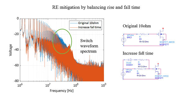
The goal of this study is to understand the RE mechanism and investigate mitigation methods in consumer electronic devices. The LED driver board in a commercial LED projector is studied. The LED driver consists of 5 boost converters. The switching noise of boost converters are measured and modeled. The GND noise of the driver board is also analyzed. Three RE mitigation methods are investigated: 1. Adding decoupling capacitors at the driver output; 2. Increasing the gate resistor; 3. Adding ferrite beads between primary ground and secondary ground. Measurements are done to show the effect of these mitigation methods. Simulation models are also built to model the switching noise and ground noise. Further RE modeling methods for this LED driver will be continuously developed and improved by the EMC Laboratory, Missouri S&T.